The LMS7002M is a dual transceiver containing just about everything you would want in a radio. Programmable clocking and synthesizers, built-in ADCs and DACs, highly configurable signal processing chains with interpolation and decimation. Capturing this into a higher-level user driver means taking on an intimate understand of this extremely flexible, and highly complex part. So how does one get started?
Fortunately, the LMS7002M is organized into separate sections with well defined boundaries. And the diagrams for each section clearly point out which registers are responsible for control for the components within the section at hand. The driver development basically mirrors these sections. So, starting with one section at a time, I began working with the external data IO interfaces, clock generation, and gradually pushing my way into the direction of the RF sections. Now, the new C driver may not initially cover all of the LMS7002M capabilities, but because the driver is organized into well-defined sections, there is a very structured way for anyone to come along and to add new functionality to the driver.
There are 1000s of registers spread across a 16 bit address field, many of which are actually shadow registers, duplicated for the dual channels A and B. To avoid careless mistakes involving bit shifts and masks, this part of the code is completely generated. So, I went through the painful task of manually transcribing the register map into a JSON format which I used to generate a data structure for all registers, and utility functions to pack and unpack these registers into the 16 bit formatting used inside the LMS7002M. This makes the code a great deal cleaner and easier to spot errors. I only wished that lime had provided some sort of register spreadsheet (or PDF that could be copied with table order intact) to simplify this transcribing step.
I have had my share of adventures discovering typos in the data sheets and magic registers, and I am sure there are more to come. However, this one really threw me off and I initially thought it was a typo. So, for the most part, receive and RX mean antenna to baseband, and transmit and TX mean baseband to antenna. So it really caught me off-guard when the data sheet used the same terms in reverse for the external data interface. The output data interface for the LMS7002M is called TX because its transmitting “receive” data from the RFIC to the BBIC (and vice-versa). Its typical to run into these sort of naming-perspective problems when dealing with flows of data. I think using a naming convention like RF2BB and BB2RF could help clear things up.
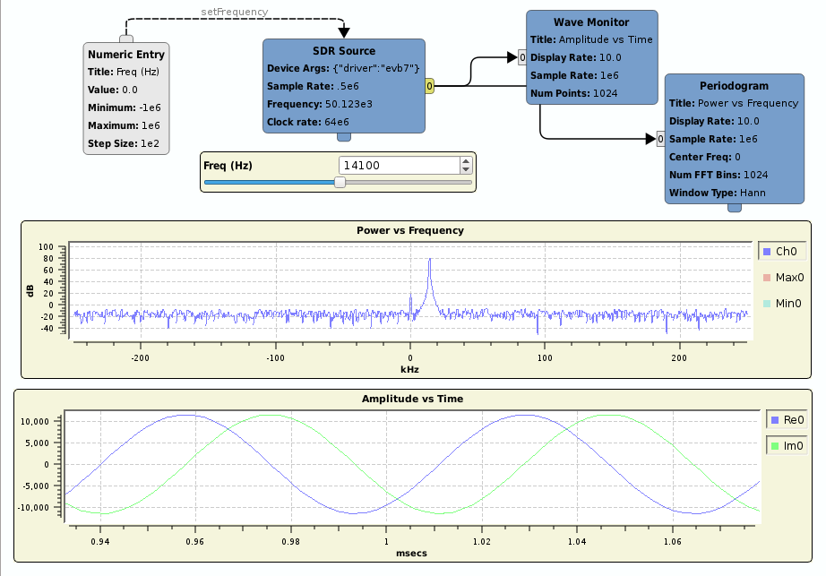
So at this point in time, I have the EVB7 evaluation board for the LMS7002M hooked up to a MicroZed through a FMC carrier card. I have interfaced the Zynq FPGA to the LMS7002M TX and RX data interfaces. There is a SoapySDR wrapper in the works that demonstrates how to configure the LMS7002M using the new C driver. Teaser screenshot attached of the LMS7002M streaming RX data from its internal test signal generator.
More great progress to come!
For further details see the LMS7002M Control Driver project page.