This is the second in a series of posts on the LimeSDR platform, that aim to demystify using SDR in the real world and programming a simple example with confidence, through bite sized chunks.
Last time we explored what the LimeSDR is and what it can achieve. In this article we will look into the LMS7002M and the RF input/output, which is where a lot of the magic (otherwise known as RF) happens.
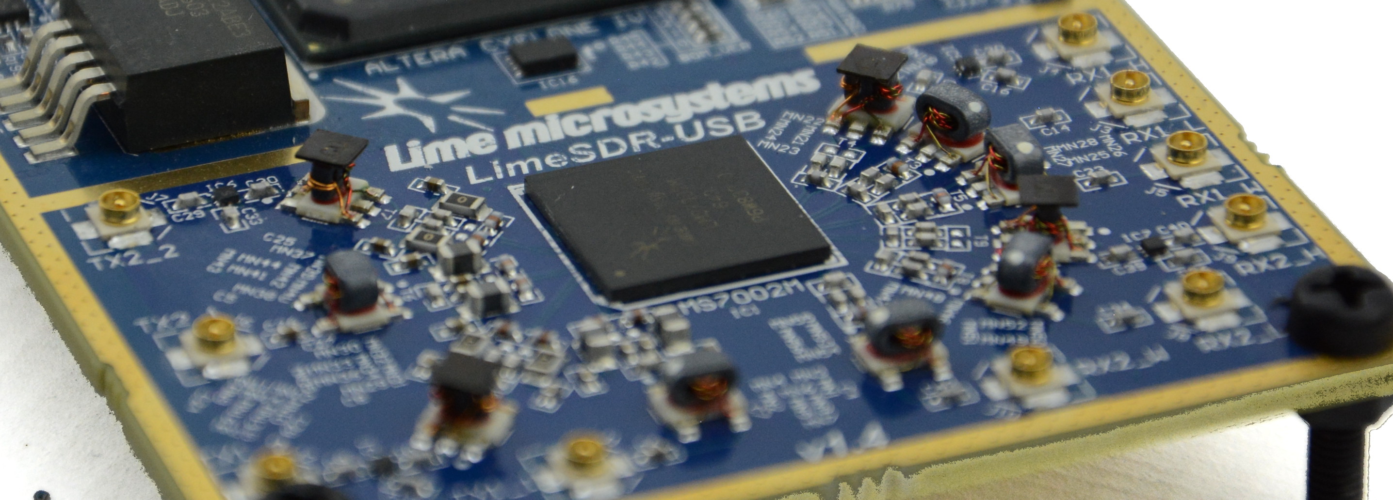
We also discussed the multiple RF connections and the underlying reason these are required. Before we dive too deep into the inner workings of the LMS7002M, we need to re-visit these inputs and outputs and consider the difference between them. The best place to start is the schematic. For simplicity we will only look at a single RF stage (there are two identical stages within the Lime/LMS7002M e.g. TX1_2 and TX2_2 are the same).

If you are not familiar with schematics or even have familiarity with them but not with RF, the RF circuit can be very daunting due to the number of discrete parts that seemingly do very little. However, using a little know-how and looking at them in a different way to the norm it’s quite easy to understand what is going on. Most training material on electronics — and even when electronics is taught at university — we are implicitly taught to consider the schematic at static conditions (between on and off) and this would even include the analogue conditions. This is fine for most designs as we can ignore frequency effects and this makes things much easier to understand. The issue is that at RF frequencies other factors start to become dominant.
Introducing frequency (warning physics ahead!)
Apologies as there is about to be a little mathematics. There are a few equations that we must bear in mind: 
 and
and
These describe the impedance of both a capacitor and inductor due to frequency. While capacitative reactance decreases with frequency, inductance increases. Secondly we must note that all circuits have both capacitance and inductance. This includes cables, PCB traces and even a tiny bit of bond wire, where they are typically treated as parasitic effects (i.e. we don’t want them). From here it should be clear why making a ultra-wide frequency input stage will become an issue as these parasitics start to get in the way.
Reflections
![]()
Image credit Oleg Alexandrov from wikipedia commons
A second concept that we need to know is an effect that occurs in an electrically long transmission line. If the impedance of the source and destination do not match a part of the waveform is reflected. The amount of reflection is dependant on the mismatch and can be worked out by an equation called the reflection coefficient.
As an aside, if you wish to learn more these reflections occur at something called a “boundary condition”. This boundary condition would be where our impedances don’t match (this could be the connector/antenna or matching network).
The distance we have to consider these effects at would be determined by the electrical length (referred to as electrically long or short). The rules of thumb vary depending upon task, but as you can see the ¼ wavelength at 3GHz is very small (less than 2.5cm) and electrically short is shorter than this, so using any cable above this length must be matched! In this case the LimeSDR is probably using an antenna therefore this will need matching in the same way. In essence this is the effect the matching is there to solve.
A little knowledge goes a long way
Now the maths and physics are out of the way we can get down to understanding what the differences are in the 3 input and 2 output stages.
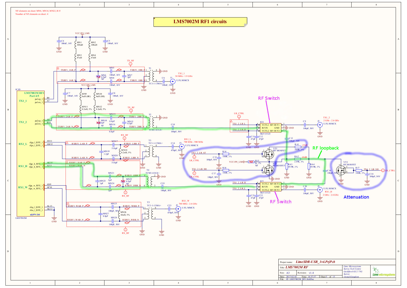
One very obvious difference in the TX1_2 and RX1_H is the MOSFETs and SKY13323 ICs. The RF loopback circuit is controlled by the switch (SKY13323 0.1-3GHz SPDT switch) and the MOSFETs (BF1105R) provide additional shunt/attenuation for the loopback stage.
If we ignore this loopback it’s easy to see the three input stages are almost the same; looking at RX1_L and RX1_W there are just a few value differences; RX1_H is almost the same but uses a non-centre tapped balun (so we can apply bias) and drops the inductor (shown as a capacitor MN22). In simplistic terms these baluns (T1-T5) turn signals from single-ended to complimentary differential and can be ignored for the purposes of understanding the input (they shouldn’t do too much to the signal).
If we look at these three stages with the topics covered in mind we can see the following:
- They will provide some filtering on the input/output that looks like a bandpass
- The impedance of these networks changes with frequency
At lower frequencies the inductor MN18/26 will look like a lower impedance across the differential pair, and as frequency increases this impedance drops and the capacitors MN17/19/20 will become more dominant. The end effect being the impedance match will change and we’ll get more reflected energy, resulting in reduced performance as we move from the “peaked” point of this circuit. The exact same occurs for the high frequency input, but the input values (MN21/24) are so small (2pf) that the parasitic inductance and capacitance will dominate the upper end of the input band and the lower will be limited by the tiny capacitors resulting in a higher frequency peaked band.
You may have a board with MN18 or MN26 removed (the HF quick fix 1). This will remove the inductor effects that the part produces towards the lower frequencies (similarly, a smaller inductor would do the same). Hopefully this post has shed some light on what this fix is doing and how it moves the matched/peaked frequencies around.
Apologies for the depth, but if we understand this concept fully it may help us to understand what is and possibly more importantly, not achievable, with each input/output. As a side note the numbers on the schematic are the “peaked” values of the networks e.g. what they are optimised for. They will work beyond these but will be dropping in performance.
The LMS7002M FPRF
In the last article we described this IC as an FPGA analogue. However, the IC does not have a gate array like a FPGA. It is an RF IC which can be reconfigured on the fly to any frequency in the 100kHz to 3.8GHz range.This class of device is referred to as an FPRF (Field Programmable RF IC), since being highly configurable it shares many of the benefits of an FPGA

The picture above shows the block diagram for the LMS7002 and from this we can see there is much inside. So what does all of this stuff do — surely it’s magic?
RF inputs (primary LNA)
As we noted there are 3 inputs and we should chose one based upon the frequency range we are working at. The LNAs (Low Noise Amplifiers) are similar in that just like the RF input stages they are peaked for specific bands.
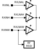
An LNA it does what is says in the name: it amplifies with low noise addition. The reason we amplify a signal early is it will give much greater immunity from noise added after amplification. If we were to inject noise (chips are noisy places) into the system before an amplifier, the noise would also be amplified, hence the reason a typical primary stage of many RF circuits is an LNA.
RF mixer
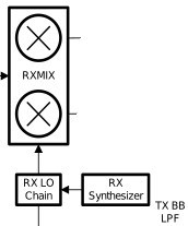
In the next stage in the receive path the signal is mixed with the RXPLL to provide a baseband (down converted) signal. The RXPLL is synthesised from the system clock via a low phase noise synthesiser. Within Lime Suite the RXPLL settings are configured from the SXR (RX synthesiser) tab. The clock which the RXPLL is synthesised from is in the CLKGEN tab (digital clock generation). This is the reason why both need to be set (we need to generate a clock via the PLL to allow us to down convert). It’s easy to overlook this step but this is a big part of the magic that allows the LMS7002M to perform it’s function.
RXTIA
Now we have down converted to baseband there is a second LNA / transimpedance amplifier.
This LNA/TIA serves multiple purposes:
- To provide a primary low pass filter of the baseband signal
- To provide some DC offset to prevent saturation of the signal, thereby preserving ADC dynamic range
- Finally, a configurable gain to condition the signal prior to filtering
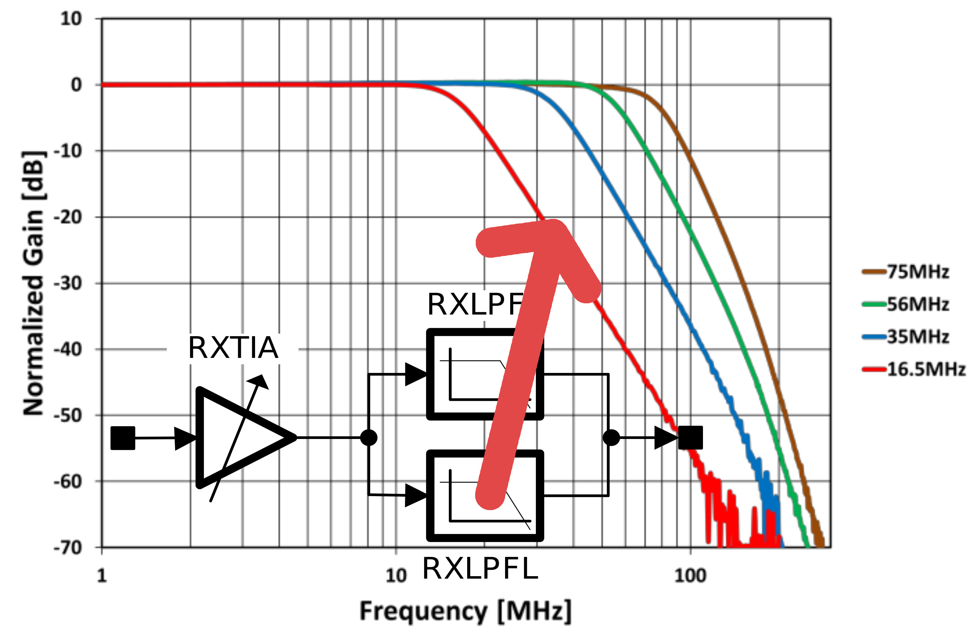
Once the signal has been though the RXTIA it is routed to either a low or high band configurable filter (RXLPFL or RXLPH). These settings live in the RFE tab of Lime Suite.
A final gain stage (RXPGA) and the ADC
There is a final LNA referred to as the RXPGA. You may be wondering why we need a third stage. Well the answer is simple but we need to look into ADC theory a little. Any ADC will have a number of bits — these are the quantisation steps and the number will be 2^ ADCbits.
For simplicity let’s assume there would be 2 bits giving 4 ADC levels (00=0V 01 =0.33V 10=0.66V 11=1V). If we want to use the full range we must have a swing of 0V to 1V. If our signal only swings 0-0.33V we would have only 1 bit of effective ADC, not the 2 bits we aimed to use and more gain is required. The same would go for too much gain and if we over drive the ADC (signal from 0.66V to 1V) we’ll have the same issue.

The RXPGA is here to solve this issue and make the signal just right for the ADC. These controls are in the RBB section of Lime Suite
But there are two of everything described — I and Q?
The output of the LMS7002M is in a form known as I (in-phase) and Q (quadrature-phase) data. This is a way of recording phase and amplitude of a signal (Q is 90 degrees out of phase of I, hence quadrature). It is very common in RF communication as it is significantly simpler than other ways of recording the same data. If you wish for some further reading National Instruments provide a white paper.
TX
For the purposes of expedience we will gloss over most of the TX at the present time to expedite getting started on some practical examples. Understanding what we have learnt about the RX and knowing the blocks are mostly just the reverse of this is sufficient for now.
If you wish to look into the TX further there are few key things to note: there is less gain required as the signals are generated at known levels, only requiring a final gain stage on the output; filtering is arguably more important on the TX as we need the best quality signals available for transmission; in addition we must also know the power we are transmitting (to stay legal in some cases or perhaps avoid over-driving an external amplifier).
Where to start
If you haven’t already get yourself a LimeSDR over at Crowd Supply
Next follow the tutorials to get Lime Suite and if required, Pothos, installed (Windows users will require the PothosSDR installer). Note at the time of writing the install instructions are in the process of being updated as a few items have changed since the tutorial was written.
Finally, follow a few examples like the Quick Test.
Final thoughts
Hopefully this post was useful and while we have skirted over the TX side, the techniques employed are very similar and we will discuss these in more depth as we delve into the software. Now we have a practical understanding of what the LMS7002M is doing we can move onto Lime Suite for the next post in the series, along with some practical tweaks to improve (and break) our applications.
Karl Woodward